As solar factories face rising material costs and pressure to shrink carbon footprints, copper metallization is appearing as a practical alternative to silver on photovoltaic cells. Copper is far cheaper per kilogram than silver and researchers have shown manufacturing paths that keep cell efficiency high while cutting the amount of silver used. The shift affects module cost, supply chains and long‑term sustainability for rooftop and utility-scale solar.
Introduction
If you follow solar prices, plan rooftop installations, or manage procurement for a project, one question is becoming practical: will the silver in solar panels stay or be replaced? Solar cells need thin metal contacts — traditionally printed with silver paste — to gather electricity. Silver works well but is costly and geopolitically concentrated at times. Researchers and manufacturers now present copper as an alternative that can lower material costs and the carbon footprint without losing much, or any, efficiency. This article looks at why copper is winning attention, how the technical change works in factories, and what it means for reliability, warranty terms and installers in the coming years.
How copper metallization works
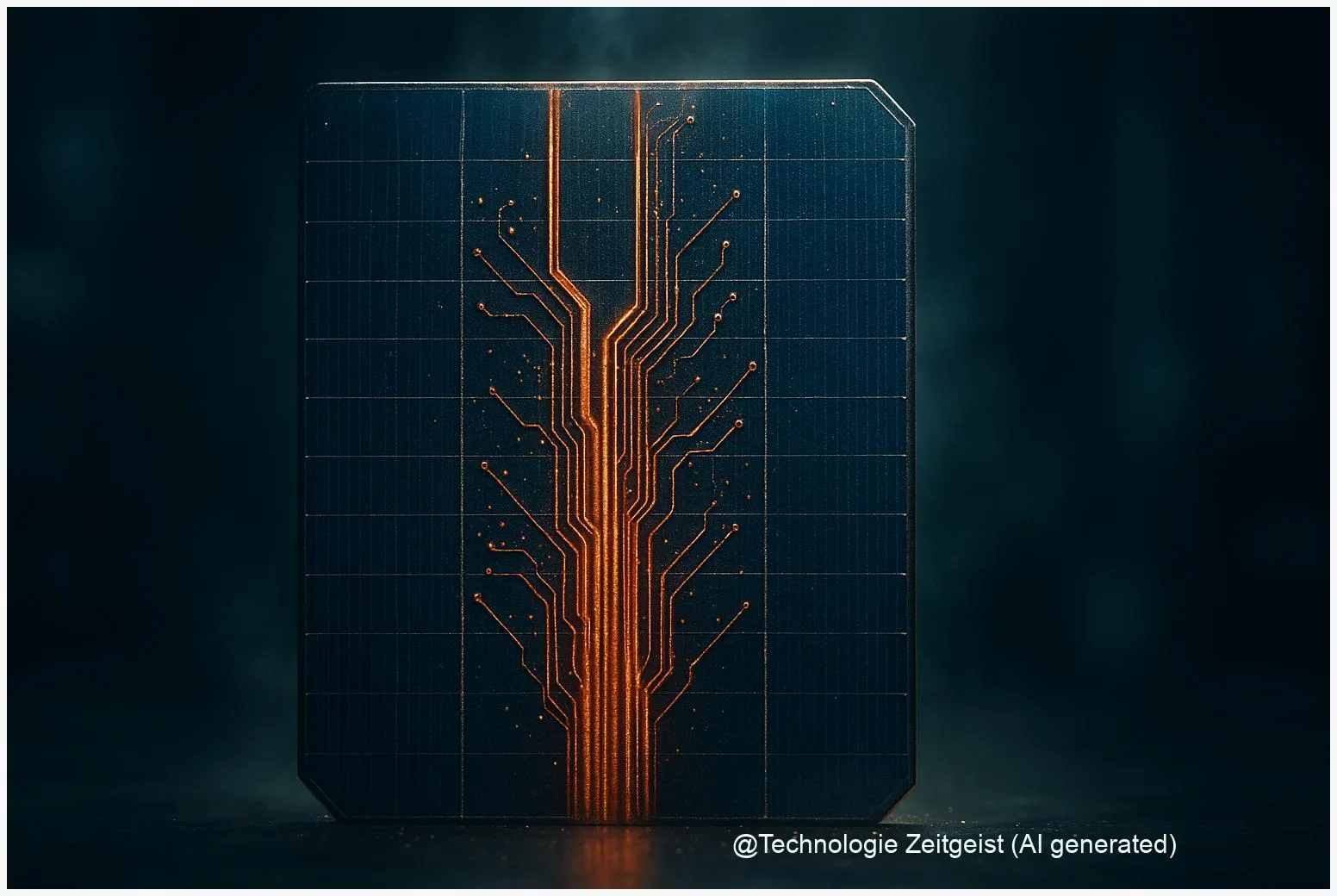
Metal contacts on a silicon solar cell form a microscopic network of fine lines and busbars. These lines must be conductive, adhere well to the silicon, and survive soldering and module encapsulation. Silver pastes became the industry standard because silver is highly conductive, resists corrosion and forms reliable contacts through a relatively mature screen‑printing and firing process.
Replacing silver is technically possible; the challenge is matching long‑term contact quality while keeping production costs low.
Copper metallization uses copper instead of silver for those printed or plated contacts. Copper has slightly higher resistivity than silver but is far cheaper and has a much lower carbon footprint per kilogram. There are three practical routes discussed in journals and institute reports:
- Ag/Cu hybrid pastes: use much less silver as a thin cap while most current is carried by copper underlayer. This reduces silver use while keeping process steps similar to current lines.
- Ni seed + Cu plating: print a nickel seed or form a thin seed layer, then deposit copper by electroplating to build low‑resistance fingers. Optionally a thin silver or tin cap improves solderability and corrosion resistance.
- Mask & plate (Mask&Plate): create an inkjet resist mask defining the finger pattern, plate copper into the openings, then remove the mask. This can produce very fine fingers and remove silver entirely on the front side.
Each route changes factory equipment or process steps: plating requires wet chemistry, mask&plate needs precise resist printing, and hybrid pastes need adapted reflow and sintering conditions. Still, laboratory and pilot demonstrations published in 2024–2025 report comparable cell efficiencies to silver references using these methods, making copper a credible candidate for broader adoption.
If a quick metric helps: many current cells use roughly 5–17 mg of silver per watt‑peak; research and pilot lines target single‑digit mg/Wp or near‑zero silver on the front side by combining plating and capping approaches.
Real‑world use and production examples
Moving from lab to factory is the key step. Several European research groups and pilot producers reported successful trials in 2024–2025. For example, the Fraunhofer ISE projects and affiliated pilot lines demonstrated SHJ (silicon heterojunction) and TOPCon cells with strongly reduced silver use by applying copper on the rear or by using plating for front contacts. Industry reporting in early 2025 described pilot‑scale shipments and improved process recipes that kept cell conversion efficiencies competitive.
In practical terms, plating is attractive for cell types that tolerate additional wet steps, while mask&plate can produce fine finger geometries that lower shading and series resistance. Large cell formats (M‑ and G‑size) used in commercial module lines have also been processed in pilot runs using copper techniques. This shows the change is not limited to small lab cells.
There are already examples in public reporting where silver use per watt has dropped substantially. Manufacturers and institutes publish incremental results: some SHJ cells reached near‑reference efficiencies with only a small silver cap left, and a handful of TOPCon pilot cells used plating to be effectively silver‑free on the front. These developments align with broader industry trends: software upgrades and new inline metrology help producers maintain yield while trying novel metallization recipes.
For further context about how rapid solar expansion changes supply and manufacturing priorities, see our coverage of recent deployment and storage trends such as the Germany 2025 solar update and long‑duration options like flow batteries, which affect grid integration and market signals for new modules (see the related TechZeitGeist pieces on Germany’s solar growth and flow batteries).
Opportunities and technical risks
Switching metals is attractive because copper costs a fraction of silver and reduces embedded emissions. On the other hand, copper brings a set of technical hurdles that factories must manage before large‑scale series adoption.
Primary opportunities:
- Lower material cost: Copper is much cheaper per kg than silver, which translates to meaningful savings at terawatt deployment scales.
- Smaller carbon footprint per kg, improving module life‑cycle emissions if supply chains are well managed.
- Potential to maintain or improve electrical performance when plating allows slimmer fingers and lower shading.
Key risks and how they are addressed:
- Diffusion into silicon: copper impurities can increase recombination in silicon if they reach the junction. Mitigations include thin nickel barrier layers, process control and encapsulation strategies.
- Corrosion and contact stability: copper oxidizes more readily than silver. Organisations use protective capping layers (tin, silver thin caps), improved encapsulation, or module‑level coatings to prevent corrosion.
- Line integration and wet chemistry: plating adds wet process steps and requires wastewater management and chemistry control; factories need to adapt floor layout and quality checks.
- Long‑term field data: IEC and other standardized ageing tests are still being accumulated for copper‑based modules; warranty frameworks may remain conservative until multi‑year field results exist.
Overall, copper solutions are reaching pilot and pre‑series readiness. Decision makers in manufacturing should require standardized long‑term tests (humidity freeze, PID, thermal cycling) and track independent field results before making irreversible line investments. For buyers and installers, the practical near‑term impact is lower material cost and potentially different handling or soldering notes in installation guides, especially if modules adopt alternative capping layers.
Where the industry may go next
Over the next few years the change is likely to be incremental rather than abrupt. Manufacturers will pilot copper routes in selected lines, then scale the ones that preserve yield and long‑term reliability. Several scenarios are plausible:
1) Hybrid adoption: Many producers will first adopt Ag/Cu hybrid pastes or thin silver caps plus copper backplane plating. This keeps process familiarity while cutting silver by a large percentage.
2) Plating scale‑up: FMCG‑style upscaling of Ni/Cu plating could become mainstream for cell lines that tolerate wet processing, enabling near‑zero silver on the front side.
3) Mask&Plate and new printing: For front contact refinement, mask&plate with resist printing or jet‑printed masks may deliver the best electrical performance and lowest silver use, but may require larger capital investments in precision printers.
What this implies for installers, buyers and policy makers: module bids and procurement documents may increasingly list the metallization route and capping materials. Policy makers and certification bodies should accelerate standardized long‑term testing so that performance warranties can adapt without raising investor uncertainty. For consumers, the benefit will likely appear as lower module prices and improved embedded carbon numbers once adoption grows.
Conclusion
Copper metallization offers a credible path to reduce material cost and carbon footprint for solar modules while keeping cell performance near current standards. Multiple technical routes — Ag/Cu hybrids, Ni/Cu plating and mask&plate — are at pilot or pre‑series readiness and have produced competitive efficiencies in laboratory and pilot lines. Remaining uncertainties centre on long‑term field behaviour, corrosion management and full process integration in large factories. Expect a staged adoption: hybrid and plating approaches first, with fully silver‑free front metallization arriving where IEC reliability tests and multi‑year field data confirm durability.
Join the discussion: share your experience with rooftop panels or thoughts about material choices for future solar systems.


Leave a Reply